文章內容
Kyropoulos Method

❒ Processing flow of KY method
Making the example of sapphire wafer, the processing flow of KY method is shown in Fig. 1 and described as follows:
1. Aluminum oxide solid is placed in a graphite crucible and heated to 2,100°C using Radio Frequency (RF) coils. The high temperature will melt the aluminum oxide solid as liquid, as shown in Fig. 1(a).
2. Using a small piece of single crystal “seed” to contact the surface of aluminum oxide liquid; pulling up the single crystal seed and rotating; then, the atoms pulled out of the liquid lever will be arranged into a single crystal structure around the seed to slowly form a small section, called “Neck,” as shown in Fig. 1(b).
3. After the solidifying speed at the junction of aluminum oxide liquid is stabilized, the seed will not be pulled up and will stop rotating. Then, by controlling the electromagnetic coil for the cooling speed, the single crystals will be gradually solidified from top to bottom to form a solid crystal column, as shown in Fig. 1(c).
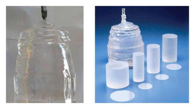
4. According to the desired atomic arrangement direction, a drill is used to drill the solid crystal column and take out the single crystal ingot, called “sapphire ingot.” It looks like a ham, as shown in Fig. 2(a).
5. Using diamond cutter to laterally slice the solid ingot into round sheets, like slicing a ham; then, polishing the surface to form sapphire wafer, as shown in Fig. 2(b).
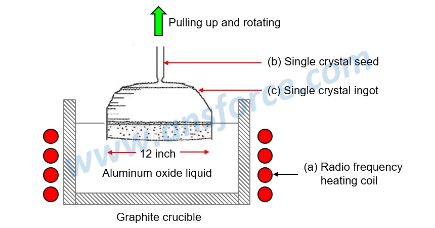
Figure 1: Processing flow of sapphire wafer.
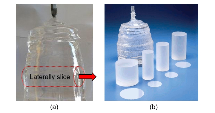
Figure 2: Appearance of Sapphire ingots and wafers
Source: www.gg-led.com、www.e-trade360.com。
❒ Advantage and disadvantage of KY method
➤ Advantage: The processing parameters of KY method is easier to control than CZ method, so normally the ceramic (metal oxide) wafers may be easily grown using KY method.
➤ Disadvantage: KY method can only produce a wafer with one atomic arrangement direction. The other directions must be obtained by lateral drilling, so the wafer area is smaller and the manufacturing cost is higher. Therefore, KY method is gradually replaced by CZ method. However, few types of wafers with complicated processing parameters and difficult production still employ KY method, such as sapphire wafer, LiNbO3 wafer, etc.
❒ Applications of KY method
The melting point of ceramic (metal oxide) wafer is higher. For example, sapphire is the aluminum oxide single crystal and the melting point of aluminum oxide is as high as 2,318K (about 2,045°C), so the temperature of aluminum oxide liquid should be as high as above 2,045°C and the crucible (pot) should be made with solid with higher melting point to accommodate such high-temperature liquid. The melting point of carbon (graphite) is 4,300K (about 4,027°C), so carbon is the most common material for making crucible. Moreover, to arrange atoms as single crystal, the condensing speed must be very slow. It will take few days to pull a single crystal ingot, so it is very energy-consuming industry. The larger the diameter of ingot is, the longer time it needs. The most commonly used wafers in the industry are:
➤ Sapphire wafer: Sapphire is the aluminum oxide single crystal and the melting point is as high as 2,318K (about 2,045°C). Sapphire contains two elements and the processing parameters are not easily controlled. Currently, the diameter of commercial wafers is 4” or 6”. The main industrial applications of sapphire wafer is to be used as the substrates of Blue LED and White LED.
➤ GaN wafer: The melting point of Gallium Nitride is as high as 2,773K (about 2,500°C), and GaN contains two elements, in which the nitrogen atom is gas, so the processing parameters are not easily controlled. GaN wafer with diameter below 2” may be produced in a laboratory, but it is still not commercialized up to now.
From the description above, we may realize that if the single crystal contains more elements, it is harder to produce, the size of ingot will be smaller, and the wafer diameter after slicing will be also smaller. If a wafer contains gas atoms, the manufacture is more difficult. GaN is the most important blue light emitting material in current commercial applications, but there is no GaN wafer available now. Then, what to do? Let’s move on!
【Remark】The aforementioned contents have been appropriately simplified to be suitable for reading by the public, which might be slightly differentiated from the current industry situation. If you are the expert in this field and would like to give your opinions, please contact the writer. If you have any industrial and technical issues, please join the community for further discussion.