文章內容
Photolithography System


❒ Principle of stepper
The lens unit in an optical exposure system will shrink the pattern on a photomask (line width about 1μm) to one tenth, so the line width projected on the Si wafer is only about 0.1μm. The ratio of line width of the pattern on a photomask to that after projection on Si wafer is about 10:1, as shown in Fig. 1. If the side length of a photomask is 50mm, the side length of a die will only be 5mm. It should be noted that the ratio used in the industry is currently 5:1 or 4:1; in other words, if the line width on Si wafer is 0.13μm, the line width on the photomask should be 0.65μm (0.13x5=0.65) or 0.52μm (0.13x4=0.52). For convenience, all the examples here utilize the ratio of 10:1 for description.
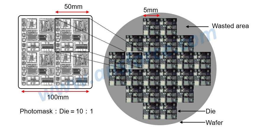
Figure 1: Ratio of photomask to die.
The machine used for photolithography technology to transfer the pattern on a photomask to Si wafer is called “stepper,” as shown in Fig. 2. Because the pattern transfer is done step by step, it is called “stepper.” The principle of stepper is similar to camera, so, in the early stage, the major manufacturers were all Japanese companies producing digital cameras, such as Canon, Nikon. Then, due to market shifting, some international integrated circuit manufacturing equipment companies dominated the market, such as ASML, Applied Materials, Lam Research. As for why these Japanese manufacturers producing digital cameras lost the market of semiconductor steppers, this is still a hot topic many industry analyzers will talk about.
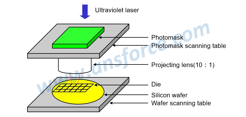
Figure 2: Photomask imaging principle of optical exposure system.
In order to accelerate the exposure speed, currently the photomask will be overlapped with many photomask patterns of the same die. As shown in Fig. 1, the four patterns on the photomask are actually the same, so four identical dies may be produced by one exposure. Because the area of Si wafer is very large (diameter of 8” or 12”) and die is usually a square with side length about 5mm, a wafer may produce hundreds or thousands of dies. Each of the dies may have millions of transistors (CMOS) thereon and every die is exactly the same. During photolithography, the photomask is placed on top of Si wafer and aligned with a certain area of Si wafer; then, irradiating ultraviolet (UV) light for exposure to form one die; after exposure, the optical scanner will move to the left about 5mm, then irradiating ultraviolet light for exposure to form the next die, as shown in Fig. 2; and, repeating this process until the whole Si wafer is formed with squares (dies) with side length of 5mm. Because the Si wafer is in a circular shape, some areas on the periphery shall be wasted, as shown in Fig. 1. Finally, by slicing these square dies, a lot of exactly the same “chips” may be obtained; after packaging and testing, the final products, i.e. integrated circuit (IC), may be obtained. Because ICs are produced in a large amount with such a technology, the cost may be reduced.
❒ Light source of stepper
The light source used by stepper is ultraviolet gas laser in high energy and high purity with concentrated beam. This kind of gas laser mostly is “Excimer laser,” which may loosen (for positive photoresist) or strengthen (for negative photoresist) the chemical bonds of photoresist. The most commonly used wavelengths of UV light are:
➤G-line: Using excimer gas laser to emit UV light with wavelength of 436nm.
➤H-line: Using excimer gas laser to emit UV light with wavelength of 405nm.
➤I-line: Using excimer gas laser to emit UV light with wavelength of 365nm.
➤KrF laser: Using KrF gas laser to emit UV light with wavelength of 248nm.
➤ArF laser: Using ArF gas laser to emit UV light with wavelength of 193nm.
➤F2 laser: Using fluorine (F2) gas laser to emit UV light with wavelength of 157nm.
The UV light with wavelength less than 300nm is called “Deep Ultraviolet” (DUV), which is currently the major light source used for IC with line width below 65nm. Using UV light with different wavelengths must be cooperated with different photoresist materials. If the wavelength of UV light is shorter, the line width of IC produced thereby may be smaller. Thus, the wavelengths of UV light used by IC steppers now become shorter and shorter.
❒ Immersion lithography
The current photolithography technology first utilizes electron beam to write the desired pattern on a quartz sheet to form a photomask; then, using projection lens to shrink the pattern on the photomask to about one tenth to be projected onto a Si wafer, wherein air will be existed between projection lens and Si wafer. Scientists found that the limit of line width this technology may reach is about 65nm, so a new technology must be used to achieve finer line width, wherein water is used to replace air that the projection lens and the Si wafer are immersed in water to let UV light first pass a layer of water. Because the refractive index of water is larger than that of air, the effect of condensation is better to focus UV light in a smaller area and reduce the line width to 45nm and even 22nm. However, with this technology, the projection lens and these precise electronic instruments must all be waterproof, and the photoresist on Si wafer must not be dissolved by water. During application, it must be very careful to avoid generating bubbles causing UV scattering.
❒ Electron beam direct write
A special electromagnetic lens may be used to concentrate the electron beam to be below 20nm for directly writing the desired pattern onto the photoresist of Si wafer, as shown in Fig. 3(a). This technology may reduce the line width of IC to be below 20nm. However, the electron beam must perform the writing one by one, so it takes a very long time. Currently, there are companies developing the technology for emitting tens of electron beams at one time, but the cost is very high and the writing speed is not fast enough. Furthermore, the electrons will be scattered back by Si wafer under the photoresist after impacting the photoresist, so the photoresist nearby which should not be irradiated by electrons may also be impacted by electrons. Therefore, the line width cannot be very small.
❒ Nano-injection lithography
This technology does not use the photomask and the photoresist, but employs the insulation material for growth to be injected by a nano-grade nozzle in a gaseous material form; and, using special electromagnetic lens to concentrate the electron beam to be below 20nm. The electron beam may break the chemical bonds of gaseous material to generate chemical reaction, so a structure with very fine line width may be directly deposited on the surface of Si wafer, as shown in Fig. 3(b). National Nano-device Laboratory in Taiwan first utilized this technology to produce IC with line width of 16nm, which is a great technology breakthrough. However, the electron beam must perform the writing one by one, so it takes a very long time. Moreover, only certain organic insulation materials may be applied for this technology, so the material selection is limited.
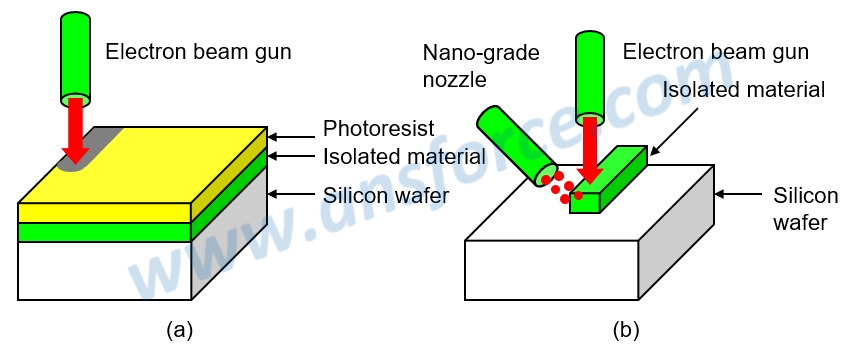
Figure 3: State-of-the-art photolithography technology.
【Example】Price of stepper
Stepper is one of the expensive machines in a foundry, Making the example of 12” 0.13μm process, the price of a stepper is about 20 million USD. The stepper using immersion lithography technology for 12” 45nm process is as high as 100 million USD. Therefore, the investment amount for a 12” foundry may be as high as 5 billion USD.
【Remark】The aforementioned contents have been appropriately simplified to be suitable for reading by the public, which might be slightly differentiated from the current industry situation. If you are the expert in this field and would like to give your opinions, please contact the writer. If you have any industrial and technical issues, please join the community for further discussion.