文章內容
Multi Metal Layer

❒ Production of multi metal layer
After applying three photomasks and many chemical reactions, the production of NMOS may be finally completed. However, this is only a completion of the basement. The following process is actually constructing the building, i.e. connecting the sources, gates and drains of those NMOS. The process for constructing building on Si wafer is called “multi metal layer.”
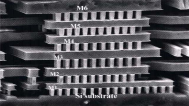
CMOS in an integrated circuit is actually a “basement.” The most important issue is to “connect” these CMOS and finally form a multi metal layer structure as shown in Fig. 1. Assuming the circled portion in the figure is MOS, the copper film will be stacked one by one thereon, sequentially from bottom to top being called Metal 1 (M1), Metal 2 (M2), Metal 3 (M3), and so on. Aluminum was used as the metal material in the early stage, so-called “Aluminum process.” Aluminum has lower melting point and is easily processed. However, the metal with low melting point is easily damaged by high temperature processing, and is also easily damaged by high temperature and electrons generated during operation of integrated circuit. Therefore, most foundries utilize the copper process, because the melting point of metal copper is higher, but is still not easily processed. Due to progress of semiconductor processing technology, the copper process is currently quite mature.
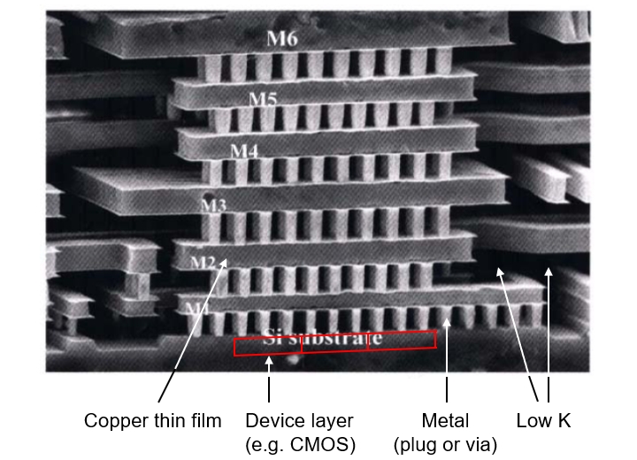
Figure 1: Multi metal layer structure of integrated circuit.
Source: United Microelectronics Corp. (UMC).
❒ Low K material
Furthermore, each of the metal layers must be separated by insulation material. This kind of insulation material is called “low K,” and is generally composed of non-conductive ceramic material or polymer material (plastic). In Fig. 1, it seems that there is no substance between each of the metal layers, i.e. being empty, but actually the low K material is dissolved by intentionally immersing the wafer in chemicals for taking the picture with three-dimensional feeling by electron microscope, so the solid low K material is truly existed between each of the metal layers. Please keep in mind that the width of these metal columns is about 0.1μm or less (actual width depending on the processing line width of the foundry), so the space between metals is impossible to be empty, otherwise all the leads in the integrated circuit might be easily damaged if the user incautiously crashed the electronic product.
It can be seen from Fig. 1 that each of metal layers is connected with “metal columns” in vertical direction. These metal columns are called “via” or “plug” and their main function is to enable electrons flowing among different metal layers along the metal columns. What is the process for producing such a complicated multi metal layer structure? The method still requires photolithography, thin film growth and etching processes.
❒ Dielectric constant
The insulation characteristic of insulation material is represented by the quantity of “dielectric constant.” The “K” mentioned above refers to the dielectric constant.
➤ High K insulation material: Indicating this insulation material may easily attract electrons and electron holes and is suitable for producing capacitors, because capacitors are originally used for storing (attracting) electrons and holes.
➤ Low K insulation material: Indicating this insulation material cannot easily attract electrons and electron holes and is suitable for producing the insulation layer between multi metal layers in Integrated Circuit (IC), so the electrons may freely flow among multi metal layers without being trapped.
As mentioned before, in the Dynamic Random Access Memory (DRAM), storing one bit of data (one 0 or 1) may be achieved with one CMOS and one capacitor. Because generally the capacitors in DRAM are made with silicon oxide and the dielectric constant of silicon oxide is not large enough (not large enough K), they cannot easily attract electrons and electron holes and thus the electrons and electron holes must be replenished periodically, so-called “Dynamic.” Once the power is turned off, the electrons and electron holes stored in the capacitor will be lost and the data stored in DRAM will be also lost. There is one type of memory, called Ferroelectric RAM (FRAM), using Lead Zirconate Titanate (PZT) and Bismuth Strontium Tantanate (SBT), i.e. insulation materials with very large dielectric constant (very large K), to produce capacitors, so as to easily attract electrons and electron holes. Thus, the data will not be lost even though the power is turned off, like portable disc (flash memory). However, the technology using ferroelectric materials, like PZT and SBT, for Si wafer processing are still mature and the cost is higher, so it is impossible to produce large-capacity memory to replace flash memory or Double Data Rate (DDR) SDRAM.
❒ Concept of multi metal layer
Assuming there are six CMOS in the “basement” need to be connected with copper wires, as shown in Fig. 2(a), i.e. connecting C1 and C2, connecting C3 and C4, and connecting C5 and C6, then how to make the connection to save the most space?
➤ Method A: As shown in Fig. 2(b), one method employs only one layer of copper wires. Because different copper wires cannot be contacted otherwise there will be short-circuit occurred to burn CMOS, all copper wires must be re-routed. If there are one million of CMOS in the basement, it is not hard to imagine how complicated circuit it will be!
➤ Method B: As shown in Fig. 2(c), another method employs three layers of copper wires, wherein C1 and C2 are connected through the first layer of copper wires (M1), C3 and C4 are connected through the second layer of copper wires (M2), and C5 and C6 are connected through the third layer of copper wires (M3), and each of the metal layers is separated by insulation material (Low K). Thus, there will be no short-circuit occurred between each of the metal layers, and thus there will be not complicated circuit.
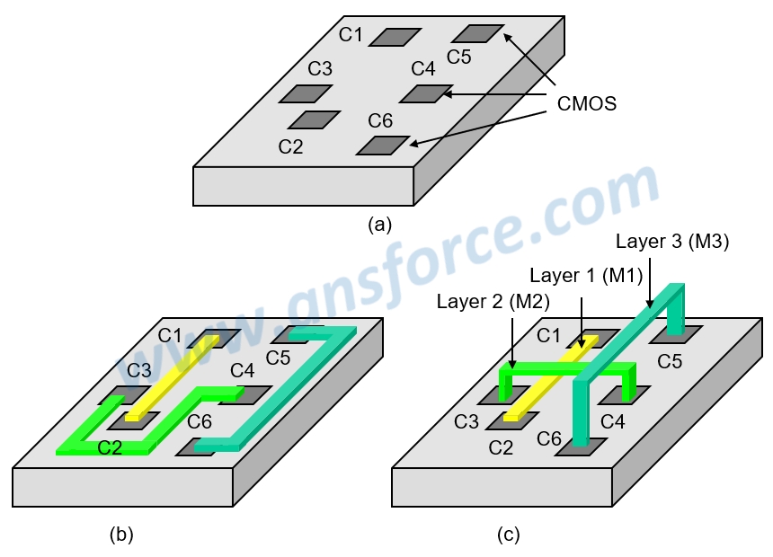
Figure 2: Multi metal layer structure of integrated circuit.
The main function of multi metal layer structure is to connect millions of CMOS in the “basement.” If there are millions of CMOS in the basement and only one layer of copper wires may be used, obviously the circuit will be very complicated and need a very large area (for isolating millions of CMOS) causing larger chip area. Thus, using multi metal layer cannot only simplify the circuit, but also keep the original area size for the chip (no need to isolate millions of CMOS). How many layers of wires (metal) are required for an IC should depend on the complexity of the IC itself; in other words, depending on the number of CMOS in the chip. If there are more CMOS, it means the chip is more complicated, the function is more powerful, so there are more layers of wires needed. Making the example of Pentium IV processor from Intel, it was made using ten layers of wires. IBM claimed to successfully produce 21 layers of wires in their laboratory. So, it might be possible to have 100 layers of wires on a silicon chip in the future. However, at least two photomasks must be added in the process for each extra layer of metal wires, wherein one photomask is used to decide the drilling locations on the low K material and another photomask is used to decide the positions of metal wires, which represents the increased cost and the difficulty of production.
❒ Number of photomasks required for producing integrated circuit
How many photomasks normally should be used to produce one Si wafer in the foundry? In the examples described herein, NMOS is made using only three photomasks, but normally CMOS will requires about eight photomasks to be produced in the foundry.
Furthermore, multi metal layer structure should be created above the CMOS to connect millions of CMOS. Therefore, the process will required about 20 photomasks in total. The line width would only be 0.1μm (only 20nm so far). It is very difficult to precisely align all the twenty photomasks. In the foundry, each photomask should be placed in the stepper; after irradiating ultraviolet light onto Si wafer, going through chemical or physical processing, such as thermal oxidation, doping, etching and film growth processes; then, the associated processes for one photomask may be completed. It will take about three days to go through the series of manufacturing processes; in other words, each photomask requires about three days completing all the associated manufacturing processes in the foundry. If one Si wafer required totally 20 photomasks, the production will need about 60 days (20 photomasks x 3 days) to be completed in the foundry.
【Remark】The aforementioned contents have been appropriately simplified to be suitable for reading by the public, which might be slightly differentiated from the current industry situation. If you are the expert in this field and would like to give your opinions, please contact the writer. If you have any industrial and technical issues, please join the community for further discussion.
【Source on article】United Microelectronics Corp. (UMC).