文章內容
Processes of Packaging and Testing


❒ Definition of Packaging and Testing
After production in foundry, Si wafer will be sealed with anti-static packing, and then sent to the packaging and testing company for packaging and testing. Because there are many packaging and testing processes to be performed alternately, except for few special cases, the packaging and testing of semiconductor will be usually conducted in the same factory to save the cost and enhance the yield rate.
➤ Packaging: Packaging chips produced by foundry with plastic, ceramic, and metal case to protect the chips from the influences of outside moisture, dust and static electricity during operation. The packaging material must consider the cost and heat dissipation effect.
➤ Testing: The produced chips must be collected for testing to test if the chips can operate normally and further confirm the reliability and yield rate of each wafer. Before packaging, the testing needs to be performed to remove the bad chips and only the good chips will be packaged and tested again after packaging, so as to check if there is any problem during packaging.
❒ Process of packaging and testing
There are many packaging and testing processes to be performed alternately and different Integrated Circuits (IC) may have different sequences. Generally, the packaging and testing processed of IC include the following steps:
➤ Testing before packaging: Before packaging, a probe card is first applied for electric testing on the dies. Fig. 1(a) shoes the appearance of a probe card. The testing for packaging of IC is to input the electric signal for testing into the bond pad via few pins of the probe card; and, then entering the CMOS within the die; after the operation by millions of CMOS, the result will be outputted via the other pins, as shown in Fig. 1(b). These outputted electric signals may be used to judge if the die can operate normally. The dies passing the test will then be packaged, and the abnormal ones will be marked with red ink.
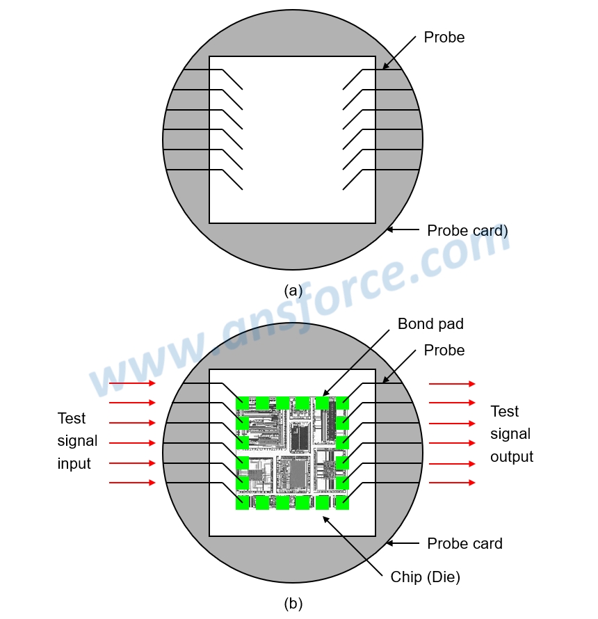
Figure 1: Using probe card for IC testing.
➤ Laser repairing and testing after repairing: Normally, a die will have memory and these dies having memory usually have “backup memory.” If the memory is malfunctioned after testing, the infrared laser will be used to cut off the corresponding metal leads. Then, the standby memory will replace the malfunctioned memory and the testing will be conducted again. If the result is good, the dies will be packaged, otherwise the dies will be marked with red ink without packaging.
➤ Die dicing and mounting: Using diamond cutter to dice dies on a wafer along the cutting line to form individual square chips; then, adhering the chips with epoxy resin inside plastic or ceramic packaging case. Epoxy resin is known as “adhesive,” so die bonding is actually fixing the dies by adhesive.
➤ Wire bonding or Flip Chip Package (FCP): Using mechanical capillary to press one end of gold wire onto the bond pad around a die and the other end onto the metal leads of a lead frame; so the electric signals may be sent to the uppermost bond pad after operation by CMOS in the basement; then, connecting gold wires with metal leads of the lead frame. Besides, the process may be applied with Flip Chip Packaging (FCP) method, which will be described in details later.
➤ Molding: Placing the chips and leads after wire bonding in a casting mold; and, injecting epoxy resin and then baking for hardening to seal the chips; the packaging case must provide the protection and heat dissipation functions. The molding operation is to completely enclose the chips to isolate from the outside moisture and contamination to protect the chips.
➤Trimming and forming: Using mechanical cutter to remove the excess epoxy resin; and trimming the plastic case into the desired shape; after trimming and forming, it will look like IC in a shape like a centipede.
➤ Pre-burn-in test: The purpose of pre-burn-in test is to ensure IC will not have short-circuit or large current during pre-burn-in to affect the operation of other normal devices and also sort out the malfunctioned ICs that these malfunctioned ICs are not required for pre-burn-in.
➤ Burn-in: Burn-in is a process to make ICs operating under very severe conditions, i.e. high temperature and high voltage, such that the malfunctioned devices may be “early failure.” For example, one IC may have some multi metal layers or metal vias that were poorly produced so it might be failed in operation for one month after shipping. If there were too many cases, the manufacturer’s credit would be damaged, and the returns may cause loss of money. Therefore, before shipping, ICs must be operating under very severe conditions, i.e. high temperature and high voltage, so they may be “early failure” and can be sorted out in advance.
➤ Final test: Final test includes a full test for specification compliance and a precise time sequence parameter test to ensure ICs can meet the shipping standard.
➤ Marking: The product information, such as manufacturer, product title, batch number, production date, is printed on the surface of packaging case by laser marking as the identification mark. Laser is a high energy beam for directly writing texts onto the packaging case.
➤ Test after packaging: The appearance of packaged IC is as shown in Fig. 2. The test after packaging for ICs is to input the electric signals for testing into IC via the metal pins on the lead frame; then, transmitting to the bond pad through gold wires; and, entering CMOS in the chip. After operation by millions of CMOS, the result will be sent out through other bond pad and transmitted to the other metal pins on the lead frame via other gold wires for output. These outputted electric signals may be used to judge if the IC can operate normally. The test after packaging is the final testing before shipping and further includes the pin scanning checking and quality assurance testing, etc. The ICs passing the tests may be shipping out for sale.
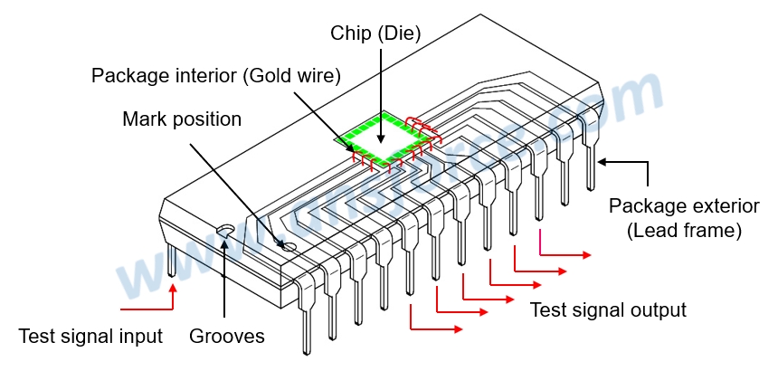
Figure 2: Integrated circuit after packaging.
【Remark】The aforementioned contents have been appropriately simplified to be suitable for reading by the public, which might be slightly differentiated from the current industry situation. If you are the expert in this field and would like to give your opinions, please contact the writer. If you have any industrial and technical issues, please join the community for further discussion.